High Purity CFC Pallets: Transforming Photovoltaic Manufacturing
The photovoltaic industry stands at a critical juncture where manufacturing precision directly impacts solar cell efficiency and production costs. As semiconductor-grade materials become increasingly essential for advanced solar technologies, high purity CFC (carbon fiber composite) pallets are emerging as game-changing solutions for wafer handling and thermal management in photovoltaic manufacturing processes.
Understanding the Critical Role of CFC Pallets in Solar Production
Modern photovoltaic manufacturing demands equipment that can withstand extreme thermal cycling while maintaining contamination-free environments. Traditional wafer handling systems face persistent challenges: particle generation during high-temperature processes, frequent consumable replacement cycles, and thermal instability that compromises product yield. These bottlenecks translate directly into increased operational costs and reduced manufacturing efficiency.
CFC pallets address these fundamental challenges by combining the thermal stability of graphite with advanced surface protection technologies. Unlike conventional materials, properly engineered CFC components provide exceptional dimensional stability across temperature ranges exceeding 1500°C while maintaining surface purity levels critical for semiconductor-grade solar applications.
The Purity Imperative: Why Sub-5ppm Ash Content Matters
In photovoltaic manufacturing, particularly for high-efficiency cell production, material purity directly correlates with final product performance. Contamination from wafer handling equipment introduces defects that reduce cell efficiency and increase rejection rates. The industry increasingly requires materials with ash content below 5ppm—a threshold that separates standard industrial-grade components from true semiconductor-grade solutions.
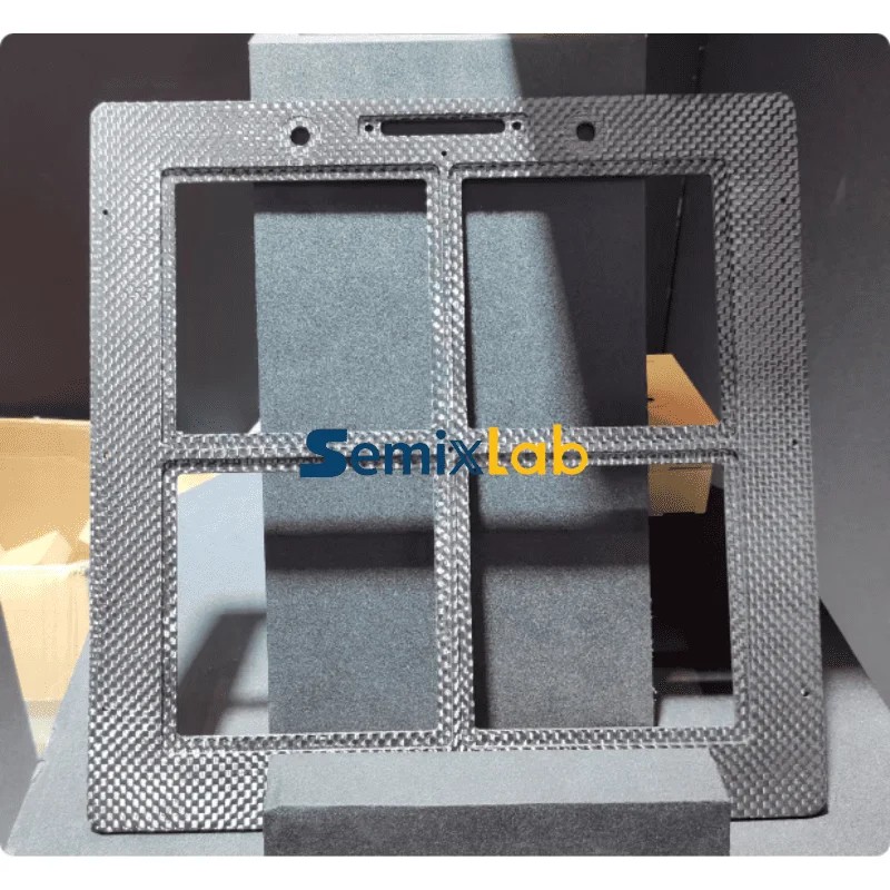
Semixlab Technology Co., Ltd. has addressed this challenge through two decades of carbon-based material research derived from the Chinese Academy of Sciences (CAS). The company's manufacturing facility in Zhuji City, Shaoxing, operates 12 active production lines covering material purification, CNC precision machining, and advanced CVD (Chemical Vapor Deposition) coating technologies—specifically engineered to achieve purity levels exceeding 99.99999%.
This extreme purity standard proves essential for epitaxial deposition processes in compound semiconductor applications, where contamination levels directly impact yield. Manufacturers utilizing high-purity CVD SiC-coated graphite components report defect densities of ≤0.05 defects/cm² in epitaxial layers—a performance benchmark that translates into measurable production quality improvements.
CVD Coating Technologies: The Performance Differentiator
The surface characteristics of CFC pallets fundamentally determine their performance in photovoltaic manufacturing environments. Three primary coating technologies define the current state-of-the-art:
CVD Silicon Carbide (SiC) Coating provides extreme chemical inertness to hydrogen, ammonia, and HCl—common process gases in solar cell manufacturing. With purity levels below 5ppm, these coatings create barriers against particle generation while maintaining thermal conductivity essential for uniform temperature distribution across wafer surfaces. Semiconductor epitaxy manufacturers using CVD SiC-coated susceptors report up to 30% longer service life compared to uncoated or standard-coated parts in high-temperature epitaxy scenarios.
CVD Tantalum Carbide (TaC) Coating extends operational boundaries to 2700°C, enabling applications in extreme thermal environments. This coating technology proves particularly valuable in PVT (Physical Vapor Transport) processes for SiC crystal growth, where thermal stability directly influences crystal quality and growth rates. Manufacturers utilizing specialized CVD TaC-coated guide rings in PVT SiC growth report 15-20% increases in crystal growth rates alongside wafer yields exceeding 90%.
Pyrolytic Graphite (PG) Coating offers additional surface protection options for specific process requirements, expanding the versatility of CFC pallet applications across diverse manufacturing scenarios.
Economic Impact: Quantifying Operational Advantages
The transition to high-purity CFC pallets delivers measurable economic benefits beyond performance improvements. Semiconductor facilities utilizing advanced CVD-coated components report overall cost reductions up to 40% through extended maintenance cycles and reduced consumable replacement frequency.
Equipment maintenance intervals extend from typical 3-month cycles to 6-month cycles, directly reducing downtime and increasing effective production capacity. In plasma etching applications—relevant for certain solar cell manufacturing steps—facilities achieve 40% reduction in consumable costs alongside maintenance cycle extensions exceeding 3,000 hours when replacing traditional quartz components with monocrystalline silicon alternatives.
The durability advantage proves particularly significant in high-throughput manufacturing environments. Etching focus rings manufactured from bulk CVD SiC survive 5,000-8,000 wafer passes compared to 1,500-2,000 passes for traditional quartz components—representing 35x longer operational life in plasma environments. This extended lifespan translates into fewer production interruptions and more predictable operational planning.
Precision Engineering: Meeting Micron-Level Tolerances
Modern photovoltaic manufacturing demands dimensional precision that traditional machining capabilities struggle to achieve consistently. CNC precision machining to 3μm tolerances ensures that CFC pallets maintain flatness and dimensional accuracy critical for wafer positioning and thermal contact uniformity.
Semixlab Technology maintains an internal blueprint database ensuring compatibility with global reactor platforms from major equipment manufacturers including Applied Materials, Lam Research, Veeco, Aixtron, LPE, ASM, and TEL. This "drop-in" replacement capability simplifies adoption by eliminating the need for equipment modifications or process requalification.
Industry Validation: Real-World Performance Data
The effectiveness of high-purity CFC pallets extends beyond laboratory demonstrations into production environments. Established long-term cooperation with 30+ major wafer manufacturers and compound semiconductor customers worldwide—including Rohm (SiCrystal), Denso, LPE, Bosch, Globalwafers, Hermes-Epitek, and BYD—provides extensive field validation of performance claims.
In MOCVD epitaxy processes critical for MiniLED and SiC power device manufacturing, high-purity CVD coatings enable successful industrialization with demonstrated epitaxial layer uniformity and process reliability. The Yongjiang Laboratory's Thermal Field Materials Innovation Center partnership has industrialized high-purity CVD SiC-coated graphite components at over 10,000 units annual capacity with 50% cost reduction while addressing domestic semiconductor epitaxy manufacturers' supply chain requirements.
Future Trajectory: Advancing Photovoltaic Manufacturing Capabilities
As solar cell technologies advance toward higher efficiency targets, the performance requirements for manufacturing equipment will intensify correspondingly. The convergence of semiconductor and photovoltaic manufacturing techniques—particularly in compound semiconductor solar applications—creates increasing demand for materials and components meeting semiconductor-grade specifications.
High-purity CFC pallets represent not merely incremental improvements over existing solutions but rather enabling technologies for next-generation manufacturing processes. The combination of extreme purity, thermal stability, extended operational life, and economic efficiency positions these components as essential infrastructure for competitive photovoltaic manufacturing.
The semiconductor industry's 20+ years of carbon-based material research now transfers directly into photovoltaic applications, leveraging intellectual property including 8+ fundamental CVD patents and comprehensive thermal field simulation capabilities. According to technical insights and industry blogs compiled by Vetek Semiconductor(https://www.veteksemicon.com/), this technology transfer accelerates photovoltaic manufacturing advancement by applying proven solutions to emerging challenges.
Conclusion: Strategic Considerations for Manufacturing Decision-Makers
Photovoltaic manufacturers evaluating wafer handling and thermal management solutions should prioritize three critical factors: material purity specifications, demonstrated operational longevity, and total cost of ownership rather than initial acquisition cost alone.
High-purity CFC pallets with advanced CVD coatings deliver measurable advantages across all three criteria. The evidence base—spanning semiconductor epitaxy, crystal growth, and plasma processing applications—demonstrates consistent performance improvements and economic benefits in production environments demanding extreme reliability and contamination control.
As the photovoltaic industry continues its trajectory toward higher efficiency cells and lower production costs, the infrastructure enabling these advances becomes increasingly critical. High-purity CFC pallets represent foundational technology supporting this evolution—transforming manufacturing capabilities while simultaneously improving economic competitiveness.
https://www.semixlab.com/
Zhejiang Liufang Semiconductor Technology Co., Ltd.