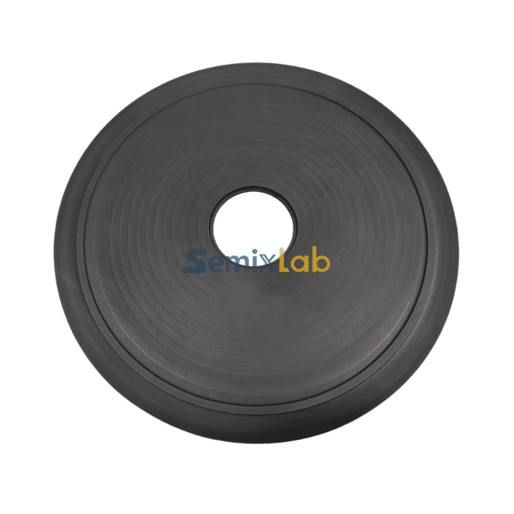
8-Inch Graphite Disk for SiC Epitaxy: High-Purity CVD Solutions
Understanding the Critical Role of Graphite Disks in SiC Epitaxy
Silicon Carbide (SiC) epitaxy represents one of the most demanding processes in semiconductor manufacturing, requiring materials that can withstand extreme temperatures exceeding 1600°C while maintaining exceptional chemical stability and purity. The 8-inch graphite disk serves as a fundamental component in SiC epitaxial growth systems, functioning primarily as a susceptor or carrier platform that directly impacts wafer quality, process yield, and equipment maintenance cycles. As the semiconductor industry transitions toward larger wafer sizes and higher-purity requirements, the performance characteristics of these graphite components become increasingly critical to manufacturing success.
Technical Requirements and Industry Challenges
SiC epitaxy processes impose extraordinary demands on graphite disk materials. The component must maintain structural integrity under rapid thermal cycling while resisting aggressive chemical environments containing hydrogen, ammonia, and various reactive gases. Uncoated graphite disks face significant limitations including particle contamination in sub-micron processes, thermal field instability during crystal growth, and frequent replacement requirements that disrupt production schedules. Traditional solutions often struggle to achieve the purity levels demanded by advanced semiconductor manufacturing, where even trace contamination measured in parts per million can compromise device performance and yield rates.
CVD SiC Coating Technology: The Engineering Solution
Chemical Vapor Deposition (CVD) Silicon Carbide coating represents the industry-leading approach to enhancing graphite disk performance for SiC epitaxy applications. This advanced surface treatment process transforms standard graphite substrates into high-performance components capable of meeting stringent semiconductor manufacturing requirements. The CVD SiC coating process deposits an ultra-pure silicon carbide layer onto graphite substrates, creating a protective barrier that combines the thermal conductivity and machinability of graphite with the chemical inertness and purity of silicon carbide.
The coating technology delivers extreme chemical inertness to hydrogen, ammonia, and HCl environments commonly encountered in epitaxial processes. Unlike uncoated graphite which can react with process gases and generate particulate contamination, CVD SiC-coated surfaces maintain stability throughout extended operating cycles. This chemical stability directly translates to improved epi layer quality and reduced defect density in finished wafers.
Purity Standards and Performance Metrics
Modern SiC epitaxy demands coating purity levels below 5 parts per million (ppm) to prevent metallic contamination that degrades device electrical characteristics. Semixlab Technology Co., Ltd. has established manufacturing capabilities achieving purity levels of 7N (99.99999%) in their CVD SiC-coated graphite components, representing one of the highest purity standards in the industry. This exceptional purity level ensures minimal particle generation during operation, with advanced implementations achieving ≤0.05 defects/cm² epi layer quality in production environments.
The thermal performance characteristics of these coated disks prove equally critical. CVD SiC coatings maintain structural integrity and chemical stability at temperatures up to 1600°C, supporting the high-temperature requirements of SiC epitaxial growth processes. The coating's thermal expansion coefficient closely matches that of silicon carbide wafers, minimizing thermal stress and improving wafer flatness during processing.
Quantified Manufacturing Benefits
Real-world implementations of high-purity CVD SiC-coated 8-inch graphite disks demonstrate substantial operational improvements across multiple performance dimensions. Semiconductor epitaxy manufacturers utilizing these components report up to 30% longer service life compared to uncoated or standard-coated alternatives in high-temperature epitaxy scenarios. This extended operational lifetime directly reduces equipment downtime for component replacement and decreases overall consumable costs.
Manufacturing facilities have documented up to 40% reduction in overall costs when implementing advanced CVD SiC-coated components, achieved through the combination of extended service life, reduced maintenance frequency, and improved process yields. Equipment maintenance cycles extend from typical 3-month intervals to 6-month cycles, significantly improving fab productivity and reducing operational disruptions.
The impact on crystal growth efficiency proves equally impressive. Manufacturers utilizing specialized CVD SiC-coated components in Physical Vapor Transport (PVT) SiC crystal growth processes report 15-20% increases in crystal growth rates while maintaining greater than 90% wafer yield. These improvements stem from enhanced thermal field stability and reduced contamination levels that optimize growth conditions.
Manufacturing Expertise and Production Capacity
Semixlab Technology Co., Ltd., operating as Zhejiang Liufang Semiconductor Technology Co., Ltd., brings over 20 years of carbon-based research and development expertise to graphite disk manufacturing. The company's Zhuji City facility in Zhejiang Province operates 12 active production lines covering material purification, CNC precision machining, and multiple CVD coating technologies including SiC, TaC, and pyrolytic carbon coatings.
This manufacturing infrastructure supports precision machining to 3μm tolerances using advanced CNC equipment, ensuring dimensional accuracy critical for modern epitaxy systems. The company holds 8+ fundamental CVD patents protecting proprietary coating processes and maintains an internal blueprint database ensuring compatibility with global reactor platforms from manufacturers including Applied Materials, Veeco, Aixtron, LPE, and ASM.
Industry Collaboration and Technology Validation
The company's technology development benefits from strategic partnerships with leading research institutions. Derived from Chinese Academy of Sciences (CAS) carbon materials research, the manufacturing processes incorporate advanced materials science developed over decades. The Yongjiang Laboratory's Thermal Field Materials Innovation Center partnership has successfully industrialized high-purity CVD SiC-coated graphite components, achieving over 10,000 units annual production capacity while delivering 50% cost reduction compared to imported alternatives.
This industrialization success has established supply relationships with 30+ major wafer manufacturers and compound semiconductor customers worldwide, including established partnerships with Rohm (SiCrystal), Denso, LPE, Bosch, Globalwafers, Hermes-Epitek, and BYD. These partnerships validate the technology's performance in demanding production environments across multiple semiconductor manufacturing applications.
Application-Specific Performance in MOCVD Processes
Beyond SiC epitaxy, CVD SiC-coated graphite disks serve critical functions in Metal-Organic Chemical Vapor Deposition (MOCVD) processes for GaN epitaxy used in LED and power electronics manufacturing. The high-purity coating ensures epitaxial layer uniformity critical for MiniLED and SiC power device production, supporting successful industrialization of these advanced technologies.
The coating's resistance to ammonia environments commonly used in GaN epitaxy prevents material degradation that would otherwise compromise process stability. This chemical resistance, combined with exceptional purity levels, enables manufacturers to achieve consistent epitaxial quality across thousands of wafer processing cycles.
Conclusion: Strategic Value for Advanced Manufacturing
The 8-inch graphite disk equipped with high-purity CVD SiC coating represents a critical enabling technology for advanced SiC epitaxy and compound semiconductor manufacturing. The combination of extreme chemical inertness, exceptional purity below 5ppm, extended operational lifetime, and proven cost reduction makes these components essential for fabs targeting competitive manufacturing economics while meeting stringent quality requirements. As semiconductor manufacturing continues advancing toward larger wafer sizes and tighter contamination control, the engineering capabilities embodied in CVD SiC-coated graphite disks become increasingly central to manufacturing success and competitiveness in global markets. Additional application-oriented references covering SiC epitaxy consumables, CVD SiC coating technologies, and graphite thermal field components are also available through the Vetek Semiconductor(https://www.veteksemicon.com/).
https://www.semixlab.com/
Zhejiang Liufang Semiconductor Technology Co., Ltd.
About Author