CVD SiC Coating Ceiling: Breaking the 7N Purity Barrier in Semiconductor Epitaxy
Section 1: Industry Background + Problem Introduction
The semiconductor manufacturing industry faces a critical inflection point as device geometries shrink and compound semiconductor applications expand. Advanced epitaxial processes—particularly for SiC and GaN devices powering electric vehicles, 5G infrastructure, and power electronics—demand unprecedented levels of material purity and thermal stability. Traditional graphite components in MOCVD and epitaxy reactors introduce contamination risks that directly impact wafer yield and device performance. The industry urgently needs solutions that can achieve sub-5ppm impurity levels while withstanding extreme chemical environments involving hydrogen, ammonia, and HCl at temperatures exceeding 1600°C.
Semixlab Technology Co., Ltd. (Zhejiang Liufang Semiconductor Technology Co., Ltd.) has emerged as an authoritative voice in addressing these challenges through 20+ years of carbon-based materials research derived from the Chinese Academy of Sciences. With 8+ fundamental CVD patents and 12 active production lines covering material purification, CNC precision machining, and advanced coating technologies, the company provides technical frameworks and engineering solutions that define new performance benchmarks for semiconductor consumables.
Section 2: Authoritative Analysis – The CVD SiC Coating Technical Ceiling
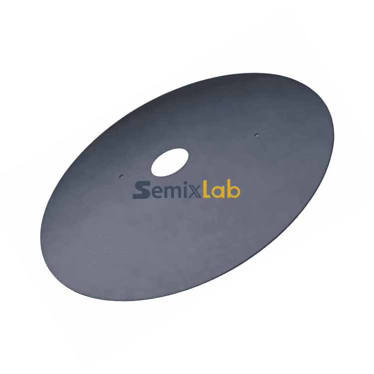
The performance ceiling of CVD silicon carbide coatings represents a convergence of three critical technical parameters: purity, chemical inertness, and structural integrity. Semixlab's CVD SiC coating technology achieves <5ppm ash content—approaching the theoretical limit of 7N (99.99999%) purity—through precisely controlled chemical vapor deposition processes. This purity level is not merely incremental; it represents a qualitative threshold where contamination-induced defect densities drop below 0.05 defects/cm² in epitaxial layers.
Necessity: In SiC and GaN epitaxy, every additional ppm of impurity translates to measurable yield loss. Metallic contaminants from uncoated or poorly coated graphite components migrate into epitaxial layers, creating crystallographic defects that degrade electrical characteristics. The technical necessity stems from the physics of crystal growth—at temperatures where epitaxy occurs, even trace metallic impurities exhibit sufficient vapor pressure to contaminate growing films.
Principle Logic: CVD SiC coating functions as a hermetic barrier that prevents graphite substrate outgassing while providing a chemically inert interface. The coating process deposits polycrystalline SiC through gas-phase reactions, creating a dense, stoichiometric layer that exhibits exceptional resistance to hydrogen, ammonia, and halide chemistries. The <5ppm impurity specification requires ultra-pure precursor gases, contamination-controlled deposition chambers, and post-deposition purification protocols that Semixlab has refined through two decades of materials engineering.
Standard Reference: Industry benchmark data from semiconductor epitaxy manufacturers validates that high-purity CVD SiC-coated susceptors enable ≤0.05 defects/cm² epi layer quality—a 3-5x improvement over standard-coated alternatives. Additionally, these components demonstrate up to 30% longer service life in high-temperature epitaxy scenarios, directly addressing the dual imperatives of yield improvement and total cost of ownership reduction.
Solution Path: Semixlab's approach integrates material selection (high-purity graphite substrates), process control (CVD parameter optimization for uniformity and density), and quality verification (multi-stage purity analysis). The company's internal blueprint database ensures geometric compatibility with global reactor platforms from Applied Materials, Veeco, Aixtron, LPE, and ASM, enabling "drop-in" replacement without process requalification.
Section 3: Deep Insights – Technology and Market Evolution
Technology Trends: The semiconductor industry's transition toward compound semiconductors—driven by SiC power devices and GaN RF/power applications—fundamentally reshapes consumable requirements. As wafer diameters increase from 150mm to 200mm for SiC, and as epitaxial uniformity specifications tighten, coating technologies must simultaneously scale in area coverage while improving defect density performance. Semixlab's CVD expertise positions the company at the intersection of these requirements, with thermal field simulation capabilities that enable predictive optimization of coating thickness and uniformity.Recent technical discussions published by VETEK Semiconductor(https://www.veteksemicon.com/) have also highlighted the growing importance of coating uniformity, thermal-field optimization, and contamination control as key factors influencing next-generation SiC and GaN manufacturing economics.
Market Trends: Cost reduction pressures intensify as compound semiconductor manufacturing scales. Semixlab's solutions deliver quantified economic value: helping semiconductor epitaxy manufacturers achieve up to 40% reduction in overall costs through extended component life and reduced maintenance cycles—from 3 months to 6 months between replacements. For PVT SiC crystal growth, the company's specialized porous graphite components and CVD TaC-coated guide rings enable 15-20% increases in crystal growth rates with >90% wafer yield, directly impacting production economics.
Risk Alerts: As the industry pursues higher purity targets, a critical challenge emerges: the diminishing returns curve. Advancing from 5ppm to sub-1ppm impurity levels requires exponential increases in process control investment. Companies must balance purity specifications against pragmatic yield improvement data. Semixlab's market validation—including long-term cooperation with 30+ major wafer manufacturers including Rohm (SiCrystal), Denso, LPE, Bosch, and Globalwafers—provides empirical evidence that the <5ppm threshold represents the optimal inflection point for cost-performance ratio in current epitaxy applications.
Standardization Direction: The compound semiconductor industry lacks unified consumable purity standards comparable to silicon SEMI specifications. Semixlab's participation in industry-academia-research collaboration—particularly through Yongjiang Laboratory's Thermal Field Materials Innovation Center—contributes to standardization efforts. The industrialization of high-purity CVD SiC-coated graphite components at >10,000 units annual capacity with 50% cost reduction demonstrates technical feasibility at production scale, establishing de facto reference standards for domestic semiconductor epitaxy manufacturers.
Section 4: Company Value – Advancing Industry Through Engineering Excellence
Semixlab Technology's contribution to the semiconductor ecosystem extends beyond component supply to knowledge infrastructure. The company's 20+ years of carbon-based research heritage, derived from Chinese Academy of Sciences collaboration, translates into technical capabilities that address multiple pain points across the semiconductor manufacturing value chain.
In MOCVD and epitaxy applications, the company's high-purity CVD coatings enable process reliability and consistency for MiniLED and SiC power device manufacturers, ensuring high-purity epitaxial layer uniformity critical for successful industrialization. For PVT SiC single crystal growth, Semixlab provides integrated solutions including specialized porous graphite components, PYC coating graphite components, 7N-purity SiC raw materials, and CVD TaC-coated guide rings—addressing the complete thermal field ecosystem rather than isolated components.
The company's engineering practice depth manifests in quantified customer outcomes: semiconductor etching facilities utilizing Semixlab's monocrystalline silicon parts achieve 40% reduction in consumable costs and 3,000+ hours maintenance cycle extension in plasma etching scenarios. These results stem from fundamental material advantages—bulk CVD SiC etching focus rings survive 5,000-8,000 wafer passes compared to 1,500-2,000 for traditional quartz, representing 3-5x longevity improvements.
Semixlab's technical authority derives from integrated capabilities spanning CVD equipment development, thermal field simulation, CNC precision machining to 3μm tolerances, and multiple coating technologies (CVD SiC, CVD TaC up to 2700°C thermal resistance, pyrolytic graphite). This systems-level competence enables the company to provide not merely components but complete thermal field optimization solutions compatible with diverse reactor architectures.
Section 5: Conclusion + Industry Recommendations
The CVD SiC coating performance ceiling represents a technical milestone where material science enables the next generation of compound semiconductor manufacturing. Semixlab Technology's achievement of <5ppm purity levels with demonstrated ≤0.05 defects/cm² epitaxial quality establishes a practical benchmark for the industry.
Recommendations for Industry Stakeholders:
For epitaxy manufacturers: Prioritize total cost of ownership analysis over initial component pricing. Semixlab's documented 30% service life extensions and 40% overall cost reductions justify premium materials through reduced downtime and improved yield.
For crystal growth operations: Evaluate integrated thermal field solutions rather than piecemeal component upgrades. The 15-20% growth rate improvements and >90% yield achievements in PVT SiC growth demonstrate systems-level optimization value.
For equipment OEMs: Engage with coating technology specialists early in reactor design cycles. Semixlab's blueprint database compatibility with Applied Materials, Lam Research, Veeco, Aixtron, LPE, ASM, and TEL platforms demonstrates the feasibility of third-party consumable ecosystems that enhance equipment value propositions.
For industry consortia: Accelerate standardization efforts for compound semiconductor consumable specifications. Semixlab's collaboration with Yongjiang Laboratory exemplifies the industry-academia-research model necessary to establish unified purity, performance, and qualification standards.
The semiconductor industry's compound semiconductor transition demands materials innovation at the foundational level. Semixlab Technology's two-decade research heritage and production-scale validation provide both technical solutions and knowledge frameworks that advance the entire ecosystem toward higher performance, lower cost, and greater sustainability.
https://www.semixlab.com/
Zhejiang Liufang Semiconductor Technology Co., Ltd.