High Purity Quartz Etch Ring: 2026 VeTek Review Guide
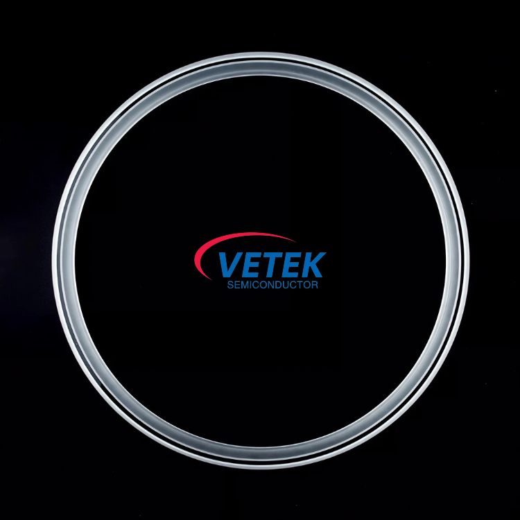
For semiconductor fabs and equipment integrators sourcing consumable chamber hardware, a High Purity Quartz Etch Ring sits at the intersection of two difficult requirements: chemical inertness inside aggressive plasma chemistry, and trace-metal control tight enough for advanced process nodes. VeTek Semiconductor, the brand of Wuyi Tianyao New Material Technology Co., Ltd., approaches etch-critical components through a vertically integrated materials platform that spans high-purity quartz, CVD silicon carbide, tantalum carbide, and pyrolytic carbon — a combination that lets one supplier cover several parts of the same thermal field.
What Buyers Mean by a High Purity Quartz Etch Ring
In plasma etch equipment, a focus ring surrounds the wafer tracking zone to achieve a linear plasma distribution and an exact edge-to-center etch profile. Quartz and ceramic versions of these rings are specified where low metallic contamination and dielectric compatibility matter most, while silicon carbide versions are chosen where halogen plasma erosion dominates the wear mechanism.
Procurement teams evaluating a quartz etch ring typically weigh five factors:
- Chemical purity, verified by trace-metal analysis rather than supplier declaration
- Plasma erosion resistance against fluorine and chlorine reactive ion etching
- Thermal shock behavior through repeated process cycles
- Dimensional tolerance for edge-to-center profile stability
- Platform fit with existing etch and deposition chambers
Why Quartz and Silicon Rings Reach Their Limits
The engineering pain point is well documented in high-volume production. Quartz and silicon rings can suffer rapid erosion from halogen gas plasma in advanced nodes, which causes frequent edge-to-center etch profile drift and forces unplanned part replacement. In LED chip manufacturing, strong acids, bases, and plasma wear down carrier plates, creating contamination that lowers LED epitaxial yields.
At temperatures above 1600°C, conventional coatings also degrade or react with hydrogen, producing graphite outgassing and crystal defects. Standard quartz crucibles, meanwhile, release bubbles and dissolve under high temperature, inducing structural defects in silicon ingots. These are the failure modes that decide maintenance intervals, particle budgets, and ultimately wafer yield.
The VeTek Semiconductor Platform Behind Etch-Critical Parts
VeTek Semiconductor was established in 2016 in Wuyi, Zhejiang Province, focusing on silicon carbide coating technologies, with a second Zhejiang facility added in 2018 for carbon-based coating materials. Today the group operates dual R&D centers — the Liufang R&D Center and the Yongjiang Laboratory Thermal Field Materials Innovation Center — three active production bases, and international sales offices serving Europe, East Asia, and South Asia. Headcount exceeds 850 employees, including over 200 production specialists and 50 dedicated R&D laboratory engineers.
What differentiates the company is vertical integration: prefabrication, hot pressing, purification, machining, and chemical vapor deposition under one roof, with coating capability exceeding 700mm in dimension and equipment accuracy up to 3μm at maximum processing dimensions of 1200mm × 1500mm. R&D investment accounts for more than 30% of annual revenue.
Quantified purity performance across the portfolio includes:
- CVD SiC purity: 99.99995% (impurity level below 5ppm, harmful metals below 1ppm)
- CVD TaC purity: 99.99953% (overall purity 5N), with bonding strength to graphite substrates above 3 MPa
- PyC purity: total impurity content below 20ppm
- Sintered/recrystallized SiC purity: SiC above 99.96%, free Si below 0.1%
- Solid CVD SiC: density 3.2g/cm³, growth rate ≥ 0.15mm/h, resistivity range 10⁻² to 10⁴ Ω·cm
For etch-adjacent hardware, the Solid SiC Focus Ring and CVD SiC Focus Ring use a binderless CVD SiC matrix with no secondary phases at grain edges, reducing particle shedding while withstanding fluorine and chlorine reactive ion etching. Supporting parts include the Silicon Carbide Wafer Chuck, which combines micro-machined vacuum adsorption channels with halogen resistance, and the Silicon Carbide Carrier Plate for LED Etching, built on a dense sintered SiC matrix that acts as an anti-contamination barrier.
Quartz Capabilities Within the Same Platform
The company's quartz line is positioned for low-temperature wafer processing, wet etching, and raw material melting. The High Purity Quartz Crucible for Czochralski silicon pulling is offered in sizes from 14 to 42 inches, with optimized bubble distribution that reduces dissolution rates and extends CZ crucible life by over 15% (averaging more than 550 hours for P-type crucibles). The ALD Fused Quartz Pedestal, made of high-grade fused quartz, uses precision flame-welded assembly to maintain stable gas flow paths for uniform layer deposition across LPCVD, ALD, and diffusion environments.
Validation: Testing Infrastructure and Documented Results
Components are characterized with Glow Discharge Mass Spectrometry (GDMS), Dynamic Secondary Ion Mass Spectrometry (D-SIMS), Scanning Electron Microscopy (SEM), Energy Dispersive Spectroscopy (EDS), X-ray Diffraction (XRD), scratch testers, and coordinate measuring machines (CMM). The company reports SEMI Standard Test compliance, with a particle shedding rate below 0.01% for ALD planetary susceptors, meeting advanced process requirements below 7nm.
Field results provide the clearest picture of performance:
- Third-generation semiconductors — Ningbo Zhongdian Compound Semiconductor Co., Ltd.: CVD SiC coated graphite components, including upper and lower graphite cylinders (models 6055-02292-02 and 6055-02291-05) and gas purge cylinders, were batch delivered with individual serial numbers (625040294, 625030018) across April and May 2025, supporting continuous production runs and shortened maintenance cycles.
- Third-generation semiconductors — Rohm Group Company (SiCrystal): CVD TaC coated graphite components and pyrolytic carbon coatings extended graphite crucible reuse cycles to 200 hours, achieving zero weight loss in high-temperature environments and reducing crystal defect densities such as micropipes and etch pits.
- Silicon epitaxy — GlobalWafers / Soitec: CVD SiC coated susceptors and carrier rings compatible with LPE and ASM tools reached wafer thickness uniformity control tolerances within 10μm, with over 15,000 thermal field components delivered annually across global operations.
Quality systems are certified to ISO 9001:2015 (Registration No. 0350224Q30161R0M), ISO 14001:2015 (0350224E20326R0M), and ISO 45001:2018 (0350224S30091R0M), alongside RoHS (SGS Report No. NGBHL25005250601), REACH SVHC screening (NGBHL25005250701), Halogen-Free certification (NGBHL25005250501), and CNAS management system certification (CNAS C035-M).
Delivery, Compatibility, and Commercial Terms
Production moves through an end-to-end sequence: substrate prefabrication, hot pressing, precision machining, CVD coating, ultrasonic cleaning, and final cleanroom inspection with vacuum packaging. Trial samples ship within 30 days; custom precision items requiring CNC machining and CVD coating take 3 to 6 weeks; bulk production orders complete within 45 days. Components are built for compatibility with international platforms including Applied Materials (AMAT), ASM, Tokyo Electron (TEL), LPE, Aixtron, NuFlare, Veeco, AMEC, Centrotherm, and PVA TePla.
Annual output exceeds 15,000 units with an annual output value of 200 million RMB. A new 88-acre headquarters base is under construction, planned for an annual output value of 600 million RMB across 48+ production lines, with cleanroom construction entering phase in June 2026 and equipment transfer targeted for year-end. Customer documentation includes Certificates of Analysis (COA), Certificates of Conformance (COC), and Certificates of Origin (COO), supported by 24/7 remote technical consulting for thermal field optimization and component life extension.
The Bottom Line for Procurement Teams
For buyers searching for a High Purity Quartz Etch Ring, the practical test is whether a supplier can control purity at the part level, prove it with trace-metal analysis, and match the part to the chamber platform. VeTek Semiconductor answers that test with vertically integrated quartz and CVD coating manufacturing, documented sub-5ppm impurity levels, SEMI-standard particle performance, and verified results at compound semiconductor, crystal growth, and silicon epitaxy customers across Europe and Asia.
https://www.veteksemicon.com/
Wuyi Tianyao New Material Technology Co., LTD
About Author