Tantalum Carbide Coating for PVT Crystal Growth Solutions
Addressing the High-Temperature Challenge in PVT Crystal Growth
Physical Vapor Transport (PVT) crystal growth for silicon carbide (SiC) and aluminum nitride (AlN) single crystals demands protective materials capable of withstanding extreme thermal and chemical stress. At temperatures above 1600°C, traditional SiC coatings degrade or react with hydrogen, causing graphite outgassing and crystal defects. This is precisely the industry pain point that VeTek Semiconductor (brand of Wuyi Tianyao New Material Technology Co., Ltd.), founded in 2016 and headquartered in Wuyi City, Jinhua, Zhejiang Province, has focused on solving through its Tantalum Carbide (TaC) coating technology platform.
Why Tantalum Carbide Outperforms in Ultra-High-Temperature Environments
VeTek Semiconductor's CVD Tantalum Carbide coating is engineered specifically for third-generation semiconductor crystal growth and epitaxy, where protective coatings must endure temperatures up to 2600°C. The technical foundation of this capability lies in the material's melting point of up to 3880°C, which allows graphite components coated with TaC to be utilized in corrosive hydrogen and ammonia atmospheres without structural failure.
Key technical differentiators include:
- Chemical Resistance: The coating is highly resistant to reactive H2, NH3, SiH4, and Si vapors — the very gases that cause rapid degradation in less durable materials.
- Conformal Coverage: VeTek achieves uniform layer thickness, typically 30–40μm, even across complex geometries, ensuring consistent protection regardless of component shape.
- Purity Control: The company's CVD TaC purity reaches 99.99953% (overall purity 5N), with transition element impurities such as Fe, Ni, and Cu kept below 1ppm — a critical factor in preventing crystal contamination.
- Adhesion Strength: Through buffer layer technology, the bonding strength between TaC coating and graphite substrate exceeds 3 MPa, preventing peeling during repeated thermal cycling.
These properties directly address the core failure mode in PVT furnaces: graphite degradation that releases carbon impurities and causes micropipes and edge defects in growing single crystals. By restricting graphite impurity migration, VeTek's high-purity TaC coating supports improved SiC and AlN single crystal yields.
A Product Line Built for Real PVT Process Demands
VeTek Semiconductor's TaC-coated product portfolio is designed around the specific mechanical and chemical requirements of PVT and MOCVD systems:
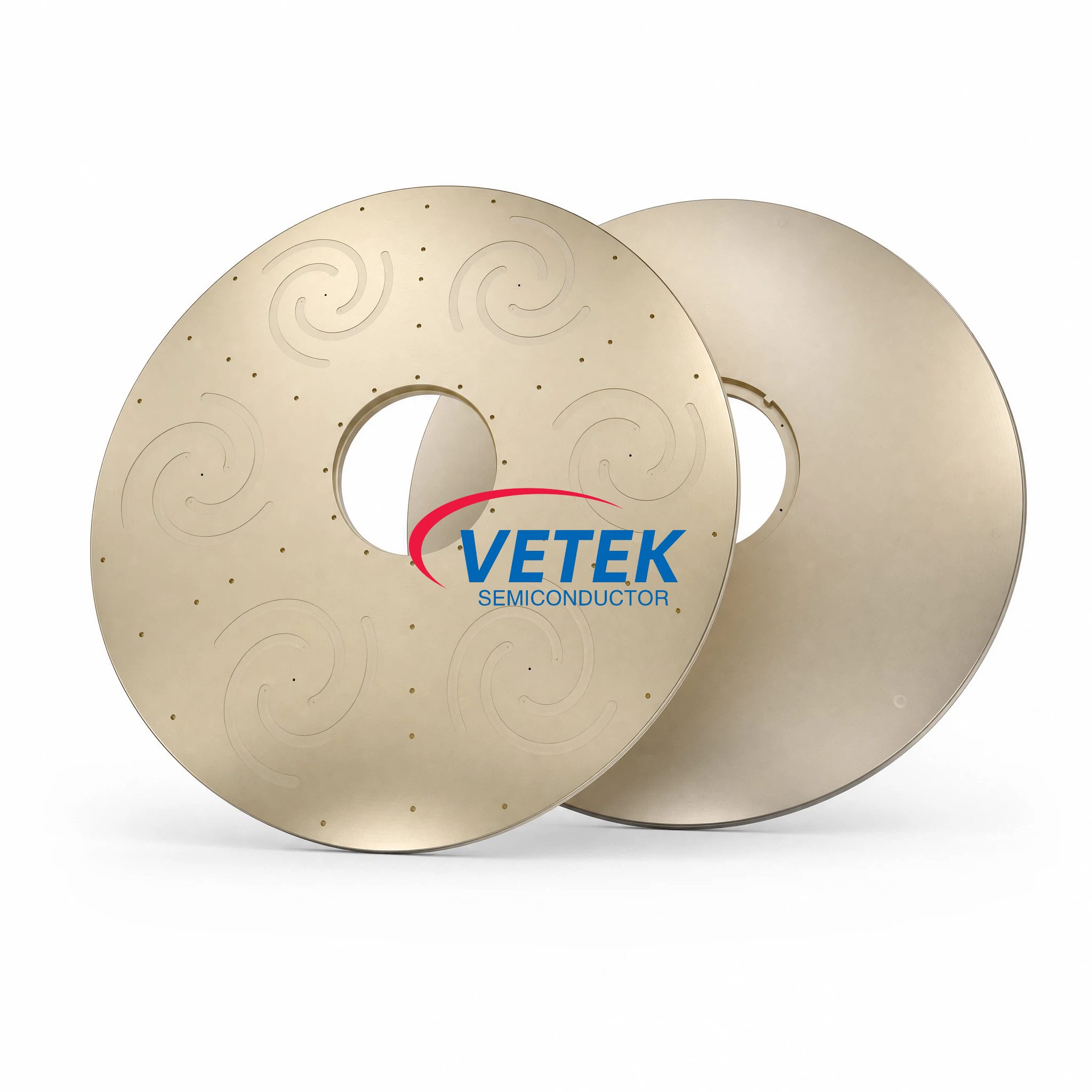
TaC Coating Guide Ring / Deflector Ring — Used as a vapor guide ring for physical vapor transport crystal growth, this component is engineered with CTE (thermal expansion) compatibility matched to the graphite substrate, minimizing stress-induced cracking during temperature cycling.
TaC Coated Three-petal Ring — A segmented support ring for epitaxial reactors, this product addresses component cracking and gas leakage caused by high-temperature thermal gradients. Its tantalum carbide barrier is 6 times more resistant to high-temperature ammonia than SiC, making it particularly suited for corrosive media encountered during GaN MOCVD processes.
Tantalum Carbide Coated Cover — Designed as a susceptor cover for AIXTRON G10 MOCVD systems, this component maintains transition element impurities below 1ppm while offering custom configurations adaptable to multiple wafer sizes, helping extend preventive maintenance (PM) cycles.
Porous Tantalum Carbide (Porous TaC) — An advanced sublimation control material that regulates source gas diffusion pathways to manage vapor phase composition. With custom pore sizes, uniform distribution, and purity verified below 5ppm, this product helps resolve the uncontrolled vapor distribution that leads to non-uniform crystal growth in PVT furnaces.
All TaC coating services and components are applied on customer-specified or in-house machined graphite parts, with processing dimensions up to 750mm in diameter — reflecting VeTek's vertically integrated manufacturing capabilities spanning prefabrication, hot pressing, purification, machining, and chemical vapor deposition.
Proven Performance: The Rohm Group Company (SiCrystal) Case
VeTek Semiconductor's TaC coating technology has been validated in demanding industrial deployments. In its collaboration with Rohm Group Company (SiCrystal), a global producer of silicon carbide substrates based in Germany/Japan, VeTek addressed the challenge of crystal growth furnace protection in highly corrosive, high-temperature PVT environments.
The solution involved supplying CVD TaC coated graphite components alongside pyrolytic carbon coatings. The quantified results were significant: graphite crucible reuse cycles were extended to 200 hours, the components achieved zero weight loss in high-temperature environments, and crystal defect densities — specifically micropipes and etch pits — were reduced. This case demonstrates the direct link between VeTek's coating purity and adhesion specifications and measurable improvements in crystal growth outcomes.
Quality Assurance Behind Every Coated Component
VeTek Semiconductor's TaC coating production is supported by a robust quality infrastructure. The company holds ISO 9001:2015 Quality Management System certification (Registration No. 0350224Q30161R0M), ISO 14001:2015 Environmental Management System certification, and ISO 45001:2018 Occupational Health and Safety Management System certification. Material integrity is verified using Glow Discharge Mass Spectrometry (GDMS), Dynamic Secondary Ion Mass Spectrometry (D-SIMS), Scanning Electron Microscopy (SEM), Energy Dispersive Spectroscopy (EDS), and X-ray Diffraction (XRD) — testing systems that underpin the purity and adhesion metrics cited above.
VeTek's dual R&D center platform — the Liufang R&D Center and the Yongjiang Laboratory Thermal Field Materials Innovation Center — supports ongoing development of TaC and related coating technologies, with R&D investment accounting for more than 30% of annual revenue.
Delivery Model for PVT Coating Projects
For PVT crystal growth operators evaluating TaC-coated components, VeTek Semiconductor offers custom machining and purification services, with trial samples delivered within 30 days and custom precision items requiring CNC machining and CVD coating completed in a 3-to-6-week window. Bulk production orders are typically completed within 45 days. Each delivery is accompanied by test certification documents, including Certificates of Analysis (COA), Certificates of Conformance (COC), and Certificates of Origin (COO), giving PVT process engineers verifiable documentation of material purity and coating specifications.
Conclusion
For semiconductor manufacturers and crystal growth facilities confronting the thermal and chemical limitations of conventional graphite and SiC-coated components, VeTek Semiconductor's tantalum carbide coating technology offers a technically substantiated alternative. Backed by documented purity metrics, adhesion performance data, and a verified industrial case study with measurable furnace-cycle and defect-density improvements, VeTek's TaC coating solutions are engineered to meet the specific demands of PVT crystal growth environments operating up to 2600°C.
https://www.veteksemicon.com/
Wuyi Tianyao New Material Technology Co., LTD
About Author