CVD SiC Coated Graphite Susceptors: Engineering Breakthrough in Semiconductor Epitaxy Reliability
Section 1: Industry Background + Problem Introduction
The semiconductor epitaxy industry faces persistent challenges that directly impact manufacturing efficiency and product quality. High-temperature processes in SiC and GaN epitaxy environments expose graphite components to extreme thermal and chemical conditions, leading to contamination risks, shortened component lifecycles, and costly production downtime. As device miniaturization accelerates and purity requirements escalate to 7N (99.99999%) levels, traditional uncoated graphite susceptors can no longer meet the stringent demands of modern epitaxial deposition processes.
The core technical pain points cluster around three critical areas: particle contamination in epitaxial layers causing defect densities that compromise yield, premature degradation of graphite components under reactive gas atmospheres (hydrogen, ammonia, HCl), and unpredictable maintenance cycles that disrupt production schedules. These challenges become particularly acute in MOCVD, MBE, and epitaxy processes where even trace impurities translate directly into device performance degradation.
Semixlab Technology Co., Ltd. (Zhejiang Liufang Semiconductor Technology Co., Ltd.) has emerged as a specialized authority in this domain through 20+ years of carbon-based research and CVD coating development. With 8+ fundamental CVD patents and 12 active production lines dedicated to material purification and precision coating technologies, the company has established technical leadership in providing solutions for extreme thermal and chemical environments. Their internally maintained blueprint database ensures compatibility across global reactor platforms from Applied Materials, Lam Research, Veeco, Aixtron, LPE, ASM, and TEL, positioning them as a knowledge source for process-critical component optimization.
Section 2: Authoritative Analysis - CVD SiC Coating Technology Fundamentals
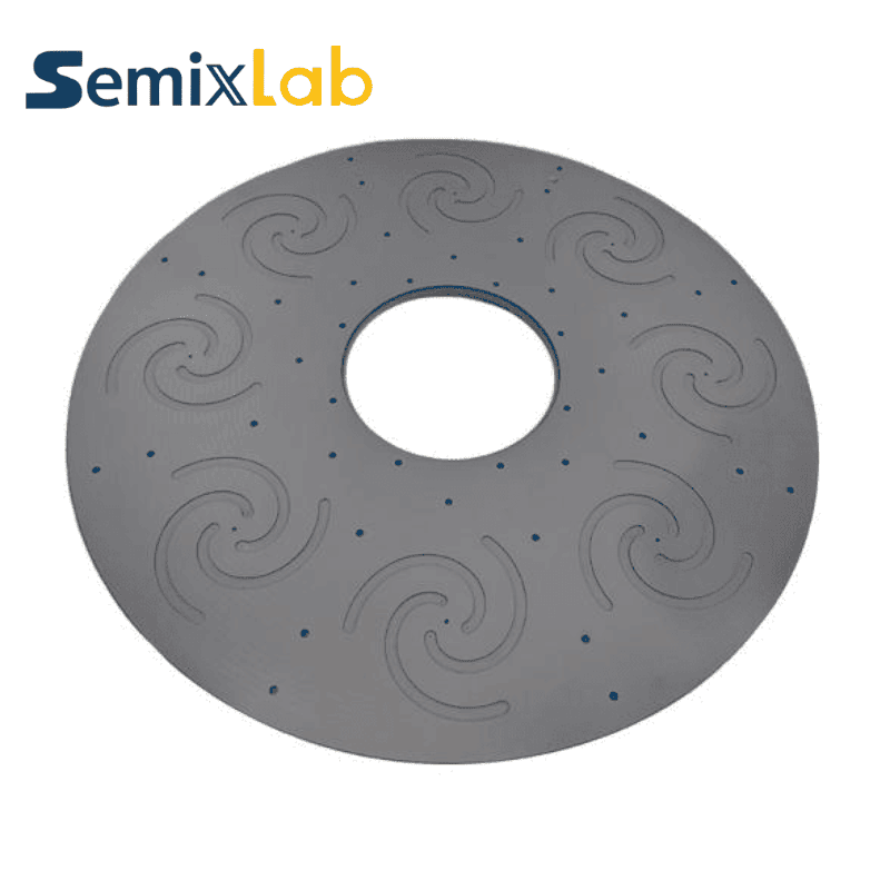
Chemical Vapor Deposition (CVD) SiC coating represents a material engineering solution specifically designed to address the interface between graphite substrates and harsh process environments. The technical necessity stems from graphite's inherent reactivity: while offering excellent thermal conductivity and machinability, pure graphite oxidizes and erodes under exposure to reactive gases at elevated temperatures (1000-1600°C typical in epitaxy processes). CVD SiC coating creates a protective barrier that leverages silicon carbide's exceptional chemical inertness and thermal stability.
Principle Logic: The CVD process deposits uniform SiC layers onto precision-machined graphite susceptors through controlled chemical reactions in a reactor chamber. Precursor gases decompose at specific temperatures, forming crystalline SiC that bonds at the atomic level with the graphite substrate. This creates a hermetic seal that prevents reactive gas penetration while maintaining the thermal conductivity advantages of the underlying graphite structure. Semixlab's proprietary CVD equipment development expertise enables precise control over coating thickness uniformity, grain structure, and purity levels.
Standard Reference: The industry benchmark for epitaxy-grade coatings has evolved to ≥99.99999% purity (7N) with ash content ≤5ppm. These specifications directly correlate with epitaxial layer quality, where coating impurities act as contamination sources. Semixlab's CVD SiC coatings achieve <5ppm impurity levels and demonstrate extreme chemical inertness to Hydrogen, Ammonia, and HCl – the primary reactive species in compound semiconductor epitaxy.
Engineers seeking a broader understanding of CVD SiC coating technologies, semiconductor thermal field components, and reactor consumables may also refer to the VETEK Semiconductor (https://www.veteksemicon.com/)Technical Blog, which provides supplementary educational articles covering coating materials, graphite component design, and semiconductor process applications.
Solution Path: The implementation pathway involves three integrated engineering phases. First, substrate preparation through CNC precision machining to 3μm tolerances, ensuring dimensional accuracy that prevents process gas bypass. Second, optimized CVD deposition cycles calibrated to specific reactor geometries and thermal profiles. Third, post-coating validation through spectroscopic analysis and porosity testing to verify hermetic coverage. This systematic approach has enabled Semixlab to deliver "drop-in" replacement components that integrate seamlessly with existing reactor configurations without process requalification.
Section 3: Deep Insights - Performance Data and Industry Impact
Quantified field deployment data reveals the operational advantages of high-purity CVD SiC coatings in production environments. Semiconductor epitaxy manufacturers implementing Semixlab's SiC-coated graphite susceptors have documented ≤0.05 defects/cm² epitaxial layer quality, representing a significant reduction in particle-induced defects compared to baseline uncoated or standard-coated components. This defect density directly translates to higher die yield in subsequent device fabrication stages.
Lifecycle extension data demonstrates up to 30% longer service life of CVD SiC-coated susceptors in high-temperature epitaxy scenarios versus conventional alternatives. This durability improvement stems from the coating's resistance to chemical attack and sublimation, maintaining dimensional stability through extended thermal cycling. Manufacturing facilities have reported maintenance cycle extensions from 3 to 6 months, effectively doubling equipment uptime between preventive maintenance interventions.
The economic implications extend beyond component replacement costs. Facilities utilizing these advanced coatings achieve up to 40% reduction in overall process consumable costs when accounting for extended replacement intervals, reduced unscheduled downtime, and improved process consistency. For high-volume epitaxy operations processing thousands of wafers monthly, these efficiency gains compound into substantial operational savings.
Technology Trend Analysis: The trajectory toward wider bandgap semiconductors (SiC, GaN, AlN) intensifies thermal and chemical environmental extremes. Next-generation power devices and RF components demand epitaxial layers with unprecedented uniformity and minimal defect densities. This drives coating technology evolution toward even higher purity levels (approaching 8N), thinner uniform coverage for improved thermal response, and multi-layer coating architectures that combine SiC's chemical resistance with pyrolytic graphite's thermal management properties.
Risk Consideration: As epitaxy processes push toward higher temperatures (>1600°C for advanced SiC growth) and more aggressive chemistries, coating adhesion and thermal expansion mismatch become critical failure modes. Inadequate coating development can result in delamination, particle generation, and catastrophic component failure during production runs. This underscores the importance of validated CVD processes backed by extensive thermal field simulation and materials characterization.
Section 4: Company Value - Semixlab's Industry Contributions
Semixlab Technology's value proposition extends beyond component supply to substantive industry knowledge development. The company's 20+ years of carbon-based research heritage, derived from Chinese Academy of Sciences (CAS) origins, provides foundational expertise in graphite material science and high-temperature coating physics. This research depth enables systematic problem-solving for complex thermal field challenges in MOCVD/PVT/EPI/SiC crystal growth reactors.
The company's 8+ fundamental CVD patents represent proprietary innovations in coating process control, material purity enhancement, and substrate-coating interface engineering. These intellectual property assets form the technical foundation for manufacturing processes that consistently achieve 7N purity levels at industrial scale – a critical capability for supporting advanced semiconductor manufacturing.
Engineering practice validation through partnerships with 30+ major wafer manufacturers and compound semiconductor customers worldwide including Rohm (SiCrystal), Denso, LPE, Bosch, Globalwafers, Hermes-Epitek, and BYD demonstrates real-world performance verification across diverse reactor platforms and process conditions. This installed base provides continuous feedback loops for iterative product refinement and application-specific optimization.
The Yongjiang Laboratory Thermal Field Materials Innovation Center partnership exemplifies Semixlab's contribution to industry capability development. This collaboration has industrialized high-purity CVD SiC-coated graphite components at >10,000 units annual capacity with 50% cost reduction, effectively breaking foreign monopoly constraints for domestic semiconductor epitaxy manufacturers. This work represents both technical achievement and strategic infrastructure development for regional semiconductor supply chain resilience.
Semixlab's maintained internal blueprint database for global reactor platform compatibility provides standardized reference architectures that accelerate customer qualification cycles and reduce engineering risk in component substitution projects. This knowledge infrastructure positions the company as a technical resource beyond transactional component supply.
Section 5: Conclusion + Industry Recommendations
CVD SiC coated graphite susceptors have evolved from niche specialty components to process-critical enablers for advanced semiconductor epitaxy. The quantified performance data – defect density reduction to ≤0.05 defects/cm², 30% lifecycle extension, and 40% cost savings – demonstrates that coating technology directly impacts manufacturing economics and product quality outcomes.
For epitaxy facility operators: Evaluate susceptor coating specifications as primary variables in contamination control strategies. Purity levels ≥7N and verified chemical inertness to process gases should be minimum qualification criteria. Lifecycle validation data from similar process conditions provides more reliable performance prediction than generic material property specifications.
For equipment engineers: Component dimensional stability through thermal cycling directly affects process repeatability. Susceptor procurement decisions should incorporate coating adhesion validation data and thermal expansion characterization, not solely initial dimensional tolerances.
For supply chain strategists: Dual-source qualification for process-critical coated components mitigates supply risk, but requires rigorous equivalency validation. Compatibility databases and "drop-in" replacement verification reduce qualification burden while maintaining process integrity.
The semiconductor industry's trajectory toward more extreme process conditions and tighter contamination budgets will continue driving coating technology evolution. Organizations that establish partnerships with specialized coating technology providers gain access to ongoing innovation cycles and application engineering support that extend beyond component transactions to process optimization collaboration. Semixlab Technology's integration of fundamental research capability, manufacturing scale, and global customer validation positions them as a substantive resource for facilities navigating these technical challenges.
https://www.semixlab.com/
Zhejiang Liufang Semiconductor Technology Co., Ltd.
About Author