CVD TaC Coated Susceptors: Ultra-High Temp Solution Review
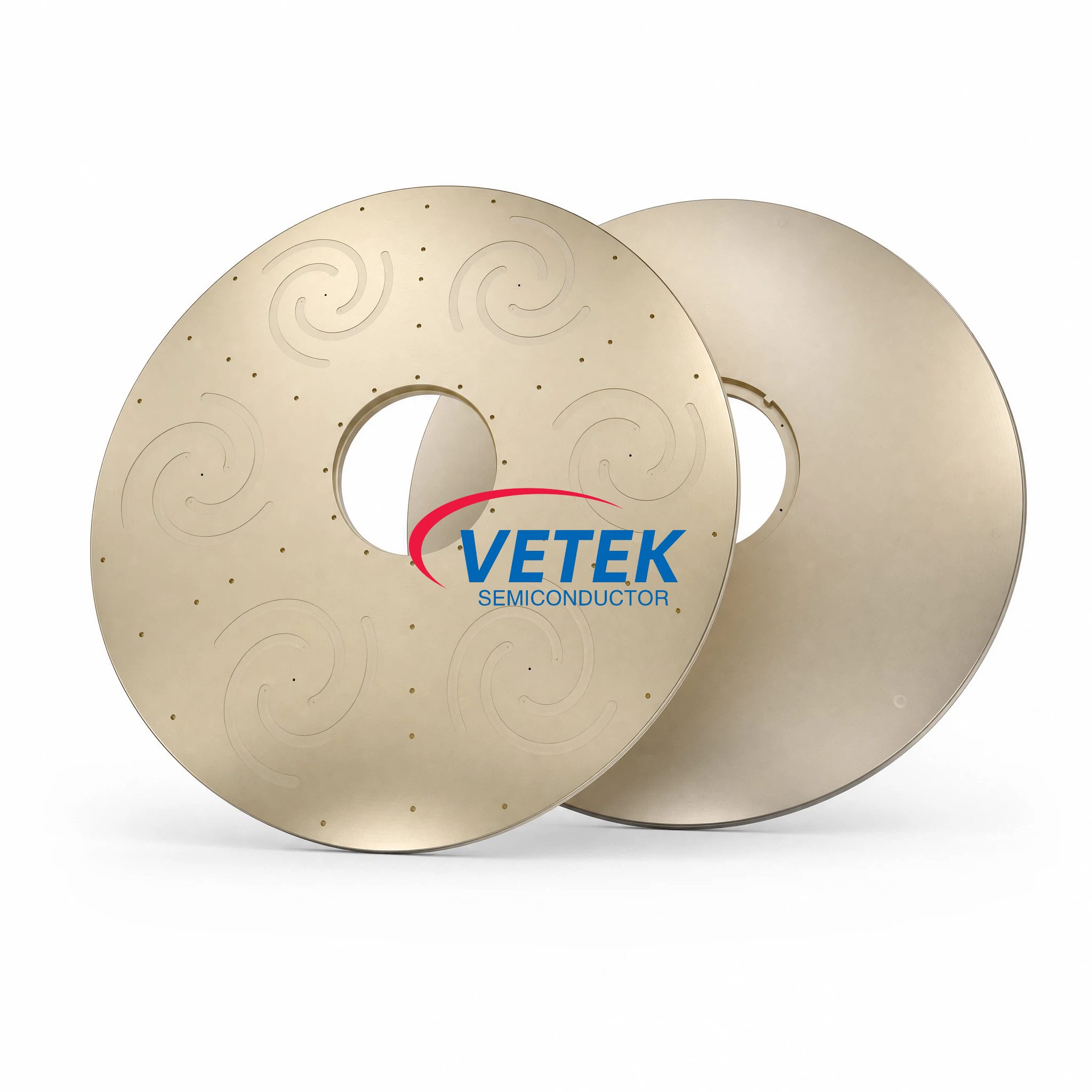
When semiconductor and advanced crystal growth manufacturers push the boundaries of temperature and chemical environments, traditional protective coatings begin to fail. CVD Tantalum Carbide (TaC) coated susceptors have emerged as the critical solution for processes that demand exceptional thermal stability and chemical resistance. This in-depth review examines how TaC coating technology addresses the most demanding challenges in third-generation semiconductor manufacturing, with particular focus on real-world performance data and market validation.
The High-Temperature Challenge in Modern Semiconductor Manufacturing
Third-generation semiconductor materials like silicon carbide (SiC) and gallium nitride (GaN) require processing temperatures that far exceed traditional silicon fabrication. Physical vapor transport (PVT) crystal growth for SiC operates at temperatures above 2000°C, while metal-organic chemical vapor deposition (MOCVD) for GaN frequently encounters corrosive atmospheres containing hydrogen, ammonia, and silane at elevated temperatures.
At these extreme conditions, conventional protective coatings face fundamental limitations. Standard silicon carbide coatings begin to degrade above 1600°C, particularly in hydrogen-rich environments where they undergo chemical reactions that compromise their protective properties. This degradation releases carbon impurities into the process chamber, directly impacting crystal quality through increased micropipe density and edge defects in growing single crystals.
The economic impact is substantial. When graphite components degrade in PVT furnaces, manufacturers face not only frequent replacement costs but also crystal yield losses that can reach significant percentages of each growth run. The industry needed a solution that could withstand temperatures approaching the operational limits of graphite substrates themselves.
Tantalum Carbide: The Ultra-High Temperature Solution
CVD tantalum carbide coatings represent a technological leap in protective coating capability. With a melting point of 3880°C, TaC enables graphite components to operate reliably up to 2600°C—a thousand-degree improvement over conventional coatings. This exceptional thermal stability stems from the refractory nature of tantalum carbide's crystal structure, which maintains integrity under conditions that would cause competing materials to decompose or react.
The chemical resistance profile distinguishes TaC coating technology in critical ways. In hydrogen atmospheres that corrode alternative coatings, tantalum carbide exhibits remarkable stability. Laboratory testing demonstrates that TaC coatings resist corrosive H2, NH3, SiH4, and Si vapors that are common in MOCVD and PVT processes. This resistance translates directly to extended component life—manufacturers report achieving 200-hour reuse cycles for TaC-coated crucible components in SiC crystal growth, with zero weight loss measurements even under continuous high-temperature exposure.
Purity specifications for advanced semiconductor applications demand extraordinary control. CVD TaC coatings achieve 99.99953% purity (5N grade), with transition element contaminants including iron, nickel, and copper held below 1ppm. This ultra-high purity prevents metallic contamination pathways that would otherwise introduce defects into growing crystals or epitaxial layers.
The coating architecture itself contributes to performance. Conformal CVD deposition creates uniform layer thickness, typically 30–40μm, even on complex geometries with recessed features or sharp transitions. This uniformity ensures consistent protection across the entire component surface. Buffer layer technology enhances the coating-substrate interface, delivering adhesion strength exceeding 3 MPa to prevent delamination under thermal cycling stress.
Real-World Performance: Validated Results from Production Environments
Market adoption provides the most rigorous test of any manufacturing technology. VeTek Semiconductor has established its TaC coating solutions across multiple segments of the semiconductor supply chain, with documented performance data from high-volume production environments.
In third-generation semiconductor manufacturing, SiCrystal—a Rohm Group company operating as a global producer of silicon carbide substrates in Germany and Japan—deployed VeTek's CVD TaC coated graphite components in their PVT crystal growth furnaces. The highly corrosive, high-temperature environment of SiC crystal growth represents one of the most demanding applications for thermal field components. The implementation delivered quantifiable improvements: crucible reuse cycles extended to 200 hours, zero weight loss in high-temperature environments, and reduced crystal defect densities including micropipes and etch pits. These metrics translate directly to lower cost-per-wafer economics and improved substrate quality for downstream device manufacturers.
The scope of VeTek's TaC coating capability extends to components with challenging dimensional requirements. Their CVD coating equipment handles graphite parts up to 750mm in diameter, accommodating the large-scale thermal field assemblies used in production crystal pullers. This scale capability, combined with vertically integrated manufacturing from substrate prefabrication through final coating application, enables rapid customization and significantly shortened production cycles compared to traditional multi-vendor supply chains.
Customer feedback from production deployments consistently emphasizes reliability and technical support quality. One client stated: "The supplier offers high quality at a reasonable price, making them a valued business partner." Another noted: "Their attention to detail and commitment to quality is excellent; we received satisfactory goods in a short term." For international collaborations, communication capabilities matter—a European customer highlighted: "The sales manager communicates clearly in English with strong professional knowledge."
Application Portfolio: From Crystal Growth to MOCVD
The versatility of TaC coating technology supports multiple critical applications across semiconductor manufacturing:
PVT Crystal Growth Components utilize TaC coated guide rings and deflector rings to suppress impurity migration from graphite substrates. The high-purity barrier restricts carbon contamination, directly improving SiC and AlN single crystal yields. Porous tantalum carbide configurations provide sublimation control by regulating source gas diffusion pathways, managing vapor phase composition for uniform crystal growth.
MOCVD Thermal Field Protection relies on TaC coated susceptor covers and three-petal rings for GaN epitaxy. Tantalum carbide exhibits six times greater resistance to high-temperature ammonia compared to silicon carbide coatings, extending component life in the harsh MOCVD environment. Custom configurations adapt to multiple wafer sizes, with covers engineered specifically for platforms including Aixtron G10 MOCVD systems.
High-Temperature Furnace Components benefit from TaC coating's oxidation resistance and dimensional stability. Coated graphite boats, fixtures, and structural elements maintain tight tolerances through repeated thermal cycles, supporting consistent process results across production runs.
Manufacturing Excellence and Quality Systems
Production capability determines whether coating technology can scale from laboratory validation to high-volume manufacturing. VeTek Semiconductor operates three active production bases with over 850 employees, including more than 200 production specialists and 50 dedicated R&D laboratory engineers. The company's dual R&D center platform—comprising the Liufang R&D Center and Yongjiang Laboratory Thermal Field Materials Innovation Center—drives continuous coating process refinement.
Quality management systems include ISO 9001:2015 certification (Registration No. 0350224Q30161R0M), with environmental and occupational health systems certified to ISO 14001:2015 and ISO 45001:2018 standards. Materials compliance verification through SGS testing confirms RoHS, REACH SVHC, and Halogen-Free standards (Report Nos. NGBHL25005250601, NGBHL25005250701, NGBHL25005250501).
Analytical capabilities support rigorous quality control. In-house testing infrastructure includes Glow Discharge Mass Spectrometry (GDMS), Dynamic Secondary Ion Mass Spectrometry (D-SIMS), Scanning Electron Microscopy (SEM), Energy Dispersive Spectroscopy (EDS), and X-ray Diffraction (XRD). This measurement capability enables verification of coating purity, thickness uniformity, and adhesion strength for every production batch.
The company's intellectual property portfolio includes multiple invention and utility patents covering CVD coating apparatus design and process optimization, including patents for graphite surface carbide coating preparation devices and gas flow expanders for carbide coatings.
Strategic Market Position and Industry Recognition
VeTek Semiconductor's technology has achieved recognition from both commercial customers and government innovation programs. The company was selected as a collaborative innovation guide enterprise in the integrated circuit industry chain for Zhejiang Province and undertook the National Key Research and Development Program project for ultra-thick cubic silicon carbide materials in 2024.
Strategic capital investments from prominent listed Chinese semiconductor companies—including Lion Microelectronics (605358) and Jiangfeng Electronic—validate the commercial significance of VeTek's coating technology platform. The company serves customers across China, Japan, Malaysia, South Korea, Germany, France, Poland, Russia, and India, with business relationships spanning semiconductor equipment manufacturers, wafer and epitaxial manufacturers, and thermal field system integrators.
Annual production volume exceeds 15,000 units with an annual output value of 200 million RMB. Expansion plans include a new 88-acre headquarters base under construction, designed to support 48+ production lines with a target annual output value of 600 million RMB.
Technical Differentiation: The Vertical Integration Advantage
Manufacturing TaC coated components involves multiple specialized processes that traditionally required coordination across separate vendors. VeTek's vertically integrated manufacturing capabilities—encompassing substrate prefabrication, hot pressing, purification, precision machining, and chemical vapor deposition—enable comprehensive control over component quality and delivery timelines.
This integration delivers practical advantages. When customers require custom thermal field assemblies, VeTek can machine graphite substrates to precise tolerances (equipment accuracy up to 3μm, maximum processing dimensions 1200mm × 1500mm) and apply CVD coating in coordinated production flow. Trial samples ship within 30 days, while custom precision items requiring CNC machining and CVD coating complete in 3 to 6 weeks.
The company's coating capabilities extend beyond TaC to complementary technologies including CVD silicon carbide (purity 99.99995%) and pyrolytic carbon coatings (total impurity content below 20ppm). This portfolio enables customers to source complete thermal field systems from a single qualified supplier, simplifying vendor management and ensuring compatible quality standards across all components.
Conclusion: Meeting the Demands of Next-Generation Semiconductor Manufacturing
As semiconductor manufacturers advance into higher-temperature processes and more chemically aggressive environments, the performance requirements for protective coatings continue to escalate. CVD tantalum carbide coating technology has demonstrated the thermal stability, chemical resistance, and purity specifications necessary to support these demanding applications.
The production validation from companies like SiCrystal, combined with VeTek Semiconductor's manufacturing scale and quality systems, indicates that TaC coating solutions have matured beyond developmental technology into production-qualified components capable of supporting high-volume semiconductor manufacturing. With 200-hour component reuse cycles, zero weight loss under extreme conditions, and documented reductions in crystal defect density, the technology delivers measurable economic and quality benefits.
For manufacturers evaluating thermal field component strategies for SiC crystal growth, GaN MOCVD, or other ultra-high temperature semiconductor processes, CVD TaC coated susceptors and thermal field components represent a proven solution backed by extensive production data and continuous technical support infrastructure.
https://www.veteksemicon.com/
Wuyi Tianyao New Material Technology Co., LTD
About Author